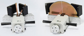
There are multiple requirements to produce fast perfect cleaving quality cross-section of crystalline materials. SELA delivered perfect cleave technology to semiconductor customers as from 2000 utilized in Perfect Cleave Mechanism (PCM) as complementary tool for automatic microcleaving systems. Hundreds of PCM units are successfully using by most of semiconductor manufacturers. As from 2014 perfect cleave capability may be your choice for sample preparation by fast perfect cleaving. Contact one of SELA’s representative for details and demo.
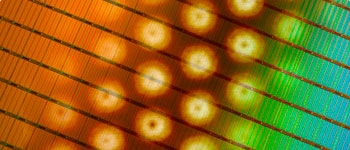
Emerging memory technology V-NAND is one of the most challenging in terms of metrology and failure analysis. Different materials and high structures of V-NAND required special techniques to ensure fastest turnaround time for sample preparation. Adaptive Ion Milling utilized in Xact200 system provides sufficient solution for delayering and cross-section of V-NAND structures in delivering wide flat areas for analysis with high accuracy end-point detection and unsurpassed quality of surface.
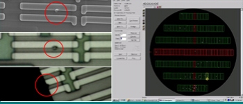
SELA provides unique solution with SELA’s Navigation SW Option which may perform navigation to specific defect on the small piece of wafer and unlike the SEM-FIB systems which may navigate on the whole wafer only as required by other navigation software packages. With SELA’s Navigation SW Option on MC600i you can easily recognize defect, navigate to defect and perform cross-section of the defect – all in one process.
Physical Failure Analysis is a process of collecting and analyzing data to determine the cause of failure. PFA plays critical role in semiconductor industry in development of new products, optimization of process parameters and improving the yield.
SELA offers sample preparation services for Physical Failure Analysis utilizing award winning state of the art technologies.
Copyright of SELA Ltd © 2018. | Terms of use
