Sela
  • Technologies
    • Nano Cleaving
    • Micro Cleaving
    • Perfect Cleaving
    • Adaptive Ion Milling ( AIM )
    • Dry sawing
    • Protected UV Masking Glue
  • Products
    • MC600i
    • MC20
    • MC10i
    • MC10
    • PCM
    • Xact200
    • EM3i
  • Services
    • SEM preparation
    • Advanced preparation
    • TEM preparation
  • Support
  • About Sela
    • Overview
    • Profile
    • Highlights
  • Careers
  • Contact Us
    • SELA contacts
    • Contact Form
  • Search
  • Menu

Xact200

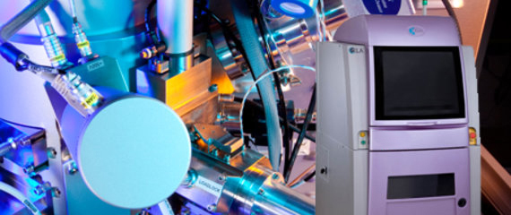
Xact200 performs cutting-edge TEM/STEM sample preparation in line with the Semiconductor and Nanotechnology roadmap requirements for next generation physical FA and characterization.

The Xact200 is a second-generation system uniquely combines the disruptive innovative AIM technology with an integrated FE SEM column, in process real time STEM imaging capability and piezo based multi axes eucentric manipulator.

The Xact200 delivers excellent sample quality, significantly reduced turn-around times and enhanced productivity.

AIM, SELA’s proprietary Adaptive Ion Milling technology, is superior to traditional Focused Ion Beam (FIB) and Broad Ion Bean (BIB) technologies in ability to reduce lamella thickness below 15 nanometers over a large area with artifact-free quality, high precision, controlled thickness variation and high throughput.

SYSTEM HIGHLIGHTS

  • Unsurpassed quality with negligible artifacts
  • Amorphous layer about 1nm on Si
  • Routine lamella thinning to below 20nm covering a wide area of interest
  • Thinning down to 10nm supporting 1x technology node
  • Enhanced lamella thickness uniformity and robustness
  • High precision milling with integrated FE SEM/STEM observation
  • AIM technology enabled by unique ion milling unit With dynamic Xe ion beam

SYSTEM FEATURES

  • Side and Plan view TEM/STEM preparation
  • Top and back side Delayering
  • SEM cross-section preparation for wide and high structures
  • SCM and SSRM preparation
  • Preparation of extremely big and extremely small objects
  • TSV and bumps SEM and TEM/STEM preparation
  • Real time STEM imaging during the milling
  • Real time thickness measurement during the milling
  • Ease of use

For additional information about SELA products please, contact us
INFORMATION REQUEST

  • MC600iOctober 15, 2018 - 10:35 am
  • MC20October 12, 2018 - 9:55 am
  • MC10iOctober 9, 2018 - 9:31 am
  • MC10May 6, 2018 - 10:07 am
  • PCMApril 6, 2018 - 8:57 am
  • Xact200March 6, 2018 - 10:05 am
  • EM3iFebruary 6, 2018 - 10:12 am

CONTACTS

SELA Ltd.
Headquarters
7 Hamada St
Southern High Tech Park
Yokneam
2069204 Israel

+972 4 827 3988

Sela USA Inc.
473 Sapena Ct,
Suite 6
Santa Clara
95054 CA
USA
+1 408 606 8189
Contact form

Copyright of SELA Ltd © 2018. | Terms of use

  • Youtube
  • LinkedIn
  • Facebook
  • Twitter
Scroll to top